- 您现在的位置:买卖IC网 > Sheet目录2008 > MAX1394ETB+T (Maxim Integrated Products)IC ADC 8BIT 416KSPS 10-TDFN-EP
MAX1391/MAX1394
Applications Information
Starting a Conversion
A falling edge on CS initiates the power-up sequence
and begins acquiring the analog input as long as OE is
also asserted low. On the 3rd SCLK falling edge, the
analog input is held for conversion. The most significant
bit (MSB) decision is made and clocked onto DOUT on
the 4th SCLK falling edge. Valid DOUT data is available
to be clocked into the master (microcontroller (C)) on
the following SCLK rising edge. The rest of the bits are
decided and clocked out to DOUT on each successive
SCLK falling edge. See Figures 8 and 9 for conversion
timing diagrams.
Once a conversion has been initiated, CS can go high at
any time. Further falling edges of CS do not reinitiate an
acquisition cycle until the current conversion completes.
Once a conversion completes, the first falling edge of CS
begins another acquisition/conversion cycle.
Selecting Unipolar or Bipolar Mode
(MAX1391 Only)
Drive UNI/BIP high to select unipolar mode or pull
UNI/BIP low to select bipolar mode. UNI/BIP can be
connected to VDD for logic-high, to GND for logic-low,
or actively driven. UNI/BIP needs to be stable for tUBS
prior to the first rising edge of SCLK after the CS falling
edge (see Figure 1) for a valid conversion result when
being actively driven.
Selecting Analog Input AIN1 or AIN2
(MAX1394 Only)
Pull CH1/CH2 low to select AIN1 or drive CH1/CH2
high to select AIN2 for conversion. CH1/CH2 can be
connected to VDD for logic-high, to GND for logic-low,
or actively driven. CH1/CH2 needs to be stable for tCHS
prior to the first rising edge of SCLK after the CS falling
edge (see Figure 1) for a valid conversion result when
being actively driven.
10
______________________________________________________________________________________
1.5V to 3.6V, 416ksps, 1-Channel True-Differential/
2-Channel Single-Ended, 8-Bit, SAR ADCs
ZS = 0
FS = VREF
1 LSB =
VREF
256
FS
FF
FE
FC
FB
00
01
03
04
OUTPUT
CODE
(hex)
INPUT VOLTAGE (LSB)
FD
0
1234
FS - 1.5 LSB
FULL-SCALE
TRANSITION
02
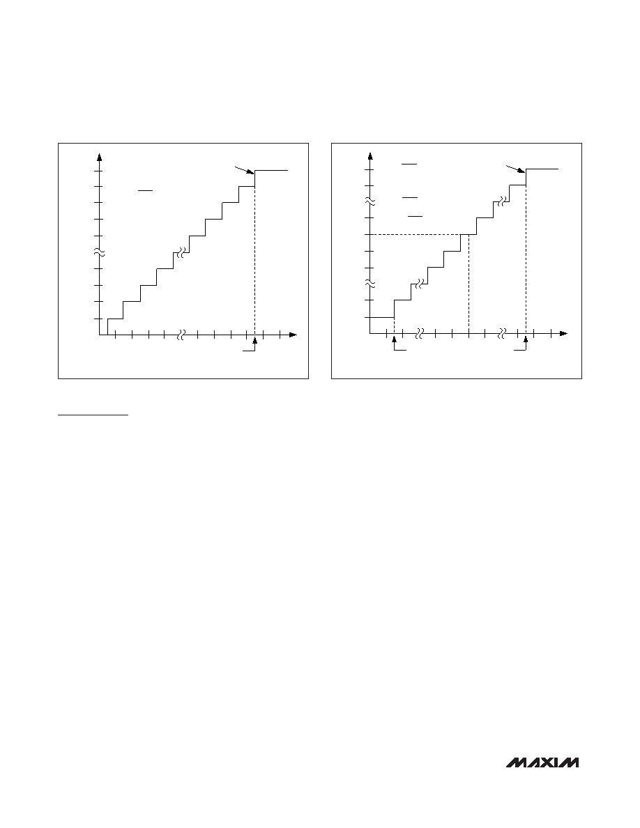
Figure 5. Unipolar Transfer Function
ZS = 0
+FS =
VREF
2
-FS =
-VREF
2
1 LSB =
VREF
256
-FS
+FS
7F
7E
01
00
80
81
FE
OUTPUT
CODE
(hex)
INPUT VOLTAGE (LSB)
FF
0
+FS - 1.5 LSB
-FS + 0.5 LSB
FULL-SCALE
TRANSITION
Figure 6. Bipolar Transfer Function
发布紧急采购,3分钟左右您将得到回复。
相关PDF资料
MAX1395ETB+T
IC ADC 10BIT 357KSPS 10-TDFN
MAX1400CAI+
IC ADC 18BIT LP 28-SSOP
MAX1401CAI+
IC ADC 18BIT LP 28-SSOP
MAX1415AEWE+T
IC ADC 16BIT DELTA SIGMA 16-SOIC
MAX1421CCM+D
IC ADC 12BIT 40MSPS 48LQFP
MAX1426EAI+T
IC ADC 10BITS 10MSPS 28SSOP
MAX1434ECQ+D
IC ADC 10BIT 50MSPS 100-TQFP
MAX1444EHJ+T
IC ADC 10BIT 40MSPS 32-TQFP
相关代理商/技术参数
MAX1394ETB-T
功能描述:模数转换器 - ADC RoHS:否 制造商:Texas Instruments 通道数量:2 结构:Sigma-Delta 转换速率:125 SPs to 8 KSPs 分辨率:24 bit 输入类型:Differential 信噪比:107 dB 接口类型:SPI 工作电源电压:1.7 V to 3.6 V, 2.7 V to 5.25 V 最大工作温度:+ 85 C 安装风格:SMD/SMT 封装 / 箱体:VQFN-32
MAX1394MTB+T
功能描述:模数转换器 - ADC 8-Bit 2Ch 400ksps 3.6V Precision ADC RoHS:否 制造商:Texas Instruments 通道数量:2 结构:Sigma-Delta 转换速率:125 SPs to 8 KSPs 分辨率:24 bit 输入类型:Differential 信噪比:107 dB 接口类型:SPI 工作电源电压:1.7 V to 3.6 V, 2.7 V to 5.25 V 最大工作温度:+ 85 C 安装风格:SMD/SMT 封装 / 箱体:VQFN-32
MAX1394MTB-T
功能描述:模数转换器 - ADC RoHS:否 制造商:Texas Instruments 通道数量:2 结构:Sigma-Delta 转换速率:125 SPs to 8 KSPs 分辨率:24 bit 输入类型:Differential 信噪比:107 dB 接口类型:SPI 工作电源电压:1.7 V to 3.6 V, 2.7 V to 5.25 V 最大工作温度:+ 85 C 安装风格:SMD/SMT 封装 / 箱体:VQFN-32
MAX1395ETB
制造商:Maxim Integrated Products 功能描述:1.5V-3.6V357KSPS1-CHANNEL TRUE-DI - Rail/Tube
MAX1395ETB+
制造商:Maxim Integrated Products 功能描述:ADC SGL SAR 357KSPS 10-BIT SERL 10TDFN EP - Rail/Tube
MAX1395ETB+T
功能描述:模数转换器 - ADC 10-Bit 2Ch 357ksps 3.6V Precision ADC RoHS:否 制造商:Texas Instruments 通道数量:2 结构:Sigma-Delta 转换速率:125 SPs to 8 KSPs 分辨率:24 bit 输入类型:Differential 信噪比:107 dB 接口类型:SPI 工作电源电压:1.7 V to 3.6 V, 2.7 V to 5.25 V 最大工作温度:+ 85 C 安装风格:SMD/SMT 封装 / 箱体:VQFN-32
MAX1395ETB-T
功能描述:模数转换器 - ADC RoHS:否 制造商:Texas Instruments 通道数量:2 结构:Sigma-Delta 转换速率:125 SPs to 8 KSPs 分辨率:24 bit 输入类型:Differential 信噪比:107 dB 接口类型:SPI 工作电源电压:1.7 V to 3.6 V, 2.7 V to 5.25 V 最大工作温度:+ 85 C 安装风格:SMD/SMT 封装 / 箱体:VQFN-32
MAX1395MTB+T
功能描述:模数转换器 - ADC 10-Bit 2Ch 357ksps 3.6V Precision ADC RoHS:否 制造商:Texas Instruments 通道数量:2 结构:Sigma-Delta 转换速率:125 SPs to 8 KSPs 分辨率:24 bit 输入类型:Differential 信噪比:107 dB 接口类型:SPI 工作电源电压:1.7 V to 3.6 V, 2.7 V to 5.25 V 最大工作温度:+ 85 C 安装风格:SMD/SMT 封装 / 箱体:VQFN-32